
High-Precision Motion and Control Solutions Enabling Maskless Lithography for PCB Manufacturing
The increasing demands for miniaturization and better functionality of electronic components and devices have a significant effect on the requirements facing the printed circuit board industry.
PCB manufacturers are being driven for producing higher density features at significantly lower costs and shorter time-to-market.
Is PCB Production with Static Mask Reaching Its Limits?
Most PCB manufacturers produce circuits board using static masks to create circuits patterns on a photoresist using a photochemical process. When manufacturing a circuit board, one of the most critical aspects is this printing and etching of the layout on the copper-clad laminates. The imaging process is central to creating a PCB layout and defines the circuit traces. The conventional imaging process needs a photographic mask called a photo-tool, photoresist covered panel, and UV light to transfer the images. The photoresist is exposed to a UV light source to harden/develop after which the PCB panel is etched with chemicals to retain the circuit pattern.
This technique is reaching its limits due to demands of creating high-density interconnects on the PCB. Creating structures that have less than 150 µm track width or spaces is becoming difficult. This leads to an increasing number of rejects. Generating of the photo tool is also a time-consuming, multi-step process.
Laser Direct Imaging or (LDI) is being considered as a possible answer for some of these challenges. LDI is a process of imaging electronic circuits directly on the PCB without the use of a photo-tool or mask. Elimination of the photo tool provides PCB manufacturers many advantages.
Laser Direct Imaging is the next step in the evolution of the PCB photolithography process. Unlike photo exposure, LDI does not employ a photo-tool. It directly exposes a digitally saved pattern onto the photo resist. LDI uses a computer-controlled laser beam to directly define circuit paths onto the board. The Photoresist is selectively exposed to the laser beam in increments across the substrate in a raster motion. The image formed can be compared to the image on a computer screen. Similar to photolithography, LDI requires a photoresist, although the resist is specially created for laser printing as LDI resist is faster-acting.
A major reason that LDI is interesting to PCB manufacturers, especially for high resolution circuits is that it eliminates the photo-tool. But what are the issues with the photo-tool? There are costs associated with the storage and preservation along with tracking and continuous inspection of a photo-tool. A photo-tool is affected by dirt, fibers, smears, and scratches which can degrade the tool and decrease the effectiveness of creating the required circuit pattern. Hence leading to rejects. A photo-tool is affected by the diffraction of light even under ideal conditions. Photo tools are also affected by temperature and humidity variations that can end up distorting the original image. You need to align mask with the substrate.

Circuit substrates and especially those used for flexible types may undergo dimensional changes when subjected to processing. In this case, a static photo-tool can be used to achieve a “best fit”, whereas in LDI the image pattern can be adjusted through the computer software for an exact fit, accommodating the dimensional changes. This is important for multilayer circuit fabrication where printing of traces, vias, and other features is critical. New PCB requirement may now require six or more layers to be aligned.
The image quality of LDI technology is clearer than that of traditional exposure methods, and hence it has obvious advantages in mid- to high-end PCB manufacturing – any distortions will reduce feature resolution.
As it doesn’t require a mask to be manufacture, it can make sense for prototyping or low volume runs.
Stage and Control Solutions Optimizing Throughput and Precision of Laser Direct Imaging
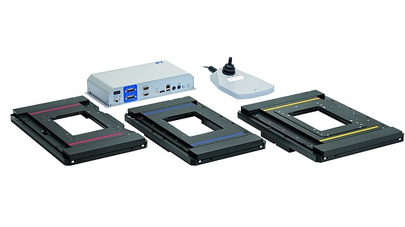
PI provides platforms and the associated controllers that meet the specific needs of machine builders in electronics manufacturing. Within a vast range of positioning systems, PI offers solutions that feature extremely low yaw error, which is essential for aligning the various focal points of the individual laser beam directions. Additionally, they also provide exceptional motion and registration accuracy and speed to meet imaging quality and throughput.
Dedicated motion controllers offer not only conventional PID algorithms, but also special algorithms that enable even higher levels of performance. For example, Motion Boost, which generates advanced motion profiles that minimize the energy fed into the stage resulting in reduced vibrations and settling times at the stepper axis. Or Servo Boost for demanding motion and settling requirements, standstill jitter and constant speed.
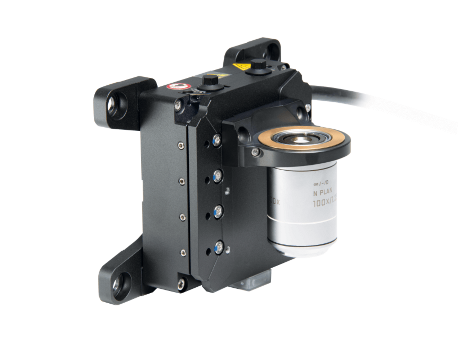
For autofocusing or focus control, PI offers Z focus stages focusers that provide fast and extended travel for multilayer PCBs. The V-308, for example, features Gaussian beam focus control for linewidth and can be used for defocusing and sharpening to optimize exposure.
PI’s engineering teams assist in combining numerous technologies and provide additional equipment, such as machine bases and software, as needed. The teams are located at many global manufacturing sites to provide responsive technical support and service for your applications.