
Electro-Optical Wafer Probing
Simultaneous Electronic Photonic Wafer-Level Testing with a Scalable Technology Platform
Next-generation devices require wafer-level test solutions capable of validating electrical and optical functions simultaneously in high-volume manufacturing contexts. Our photonic wafer probing technology unifies both domains in a fully automated workflow, combining nanometer-level optical alignment with high-density electrical probing within a compact, ATE-compatible architecture. Miniaturized photonic alignment engines with precise actuation and advanced algorithms ensure stable optical coupling while sustaining production throughput. This approach reduces the cost of test through parallel workflows and offers a scalable path to high-volume manufacturing of electronic-photonic integrated circuits (EPICs).
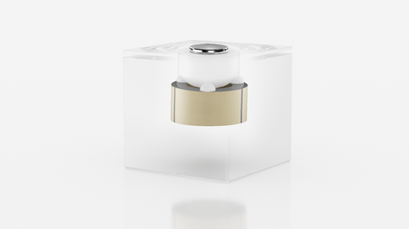
Integrated Electro-Optical Probe Architecture
Integrated Electro-Optical Probe Architecture
The platform merges high-density electrical probing with automated, miniaturized fiber-array unit (FAU) alignment. Simultaneous electrical and optical probing shortens test cycles and boosts operational efficiency. Engineered for ATE compatibility, the architecture integrates seamlessly with existing test heads, wafer handlers, and automation frameworks.
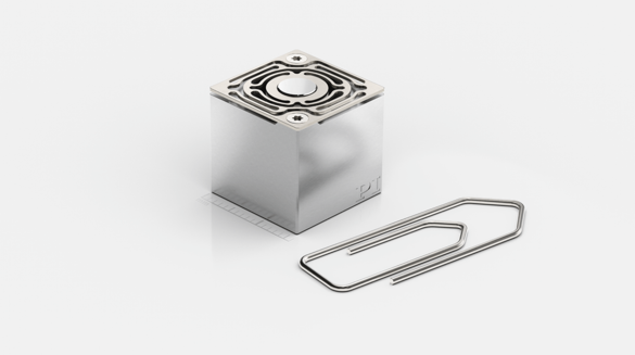
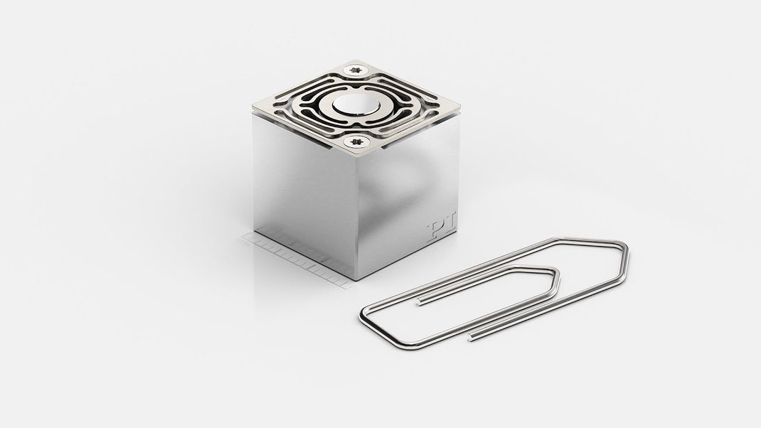
Production-Grade Photonic Alignment
Production-Grade Photonic Alignment
Our ultracompact photonic alignment engine provides nanometer-scale optical positioning in a footprint optimized for high-volume manufacturing. With multi-degree-of-freedom actuation and proprietary alignment algorithms, it achieves stable, repeatable, and fast coupling across test sites and wafers. The engine delivers production-grade throughput without the complexity of R&D-oriented alignment platforms.
Scalable Test Workflow for High-Volume Manufacturing
Scalable Test Workflow for High-Volume Manufacturing
A unified workflow orchestrates automated alignment, parallel measurements, and predictable probe-to-wafer interaction. This enables simultaneous testing and establishes a reliable foundation for yield learning, resulting in faster characterization, quicker feedback loops, and a lower cost of test as volumes scale.
Direct High-Resolution Fly-Height Measurement
Thanks to nanometer precision and millisecond-level alignment speeds, our photonic alignment engines are the fastest photonic contact systems on the market. Maintaining exact fly height, however, is critical to avoiding costly crashes. Industry-standard capacitive sensors are bulky and indirect. Our FAU ranging technology changes everything:
- Uses existing fiber channels for interferometry-based distance measurement with no extra hardware in the test interface—and no added footprint
- Measures the fiber-to-wafer distance at the point of interest
- Additional measurement channels assign distance values to each FAU, eliminating limitations resulting from averaged measurements

With FAU ranging, we pave the way for trench-based photonic edge coupling, saving wafer real estate, reducing device costs, and unlocking new design freedom for EPIC manufacturers.
Dr. Markus Simon, Strategic Innovation and Technology Management
Electro-Optical Wafer Probing: Today’s Technology, Tomorrow’s Potential
Our technology platform accelerates applications ranging from silicon photonics in datacom and telecom, optical computing and AI performance, and integrated LiDAR and 3D sensing to quantum photonics, biosensing and lab-on-chip systems, and AR/VR optical modules. Together with industry partners, our team is advancing integrated electro-optical test methodologies that support high-volume EPIC manufacturing, enabling a predictable yield ramp, consistent coupling performance, and scalable, production-grade photonic validation.
Our miniature ultrasonic tip/tilt mirror can be scaled and tailored to your optical system. Talk to our engineers about your specific requirements.
Contact us!